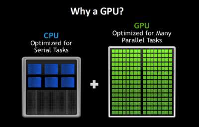
Graphics Processing Units (GPUs) were originally designed as specialized chips for rendering graphics, like making video games faster and smoother. They've since become the go-to tools for training AI models and working with massive datasets because of their ability to perform multiple tasks simultaneously (parallel processing).
NVIDIA unveiled their Blackwell GPU lineup during the GTC 2024, including the NVIDIA GB200. Recently, they released GB200 GPU, which is purpose-built for AI and high-performance computing. In this article, we will discuss the NVIDIA GB200 in detail; we'll explore its architecture and how it works in different scenarios.
You can read more about the Blackwell specifications here: NVIDIA’s Blackwell architecture: breaking down the B100, B200, and GB200.
Before we discuss the architecture of the GB200, let’s give a brief background of the general architecture of an NVIDIA GPU.
The basic architecture of NVIDIA GPUs
To understand the architecture of the GB200, it helps to have a basic grasp of how NVIDIA GPUs are generally structured. You can think of NVIDIA GPUs as a collection of specialized cores designed to work together perfectly.
These cores are grouped into Streaming Multiprocessors (SMs), which are the building blocks of the GPU. Each SM contains a set of CUDA cores and other components like cache memory, which helps the cores access data quickly and control logic that manages the instructions flow.
These CUDA cores enable the parallel processing that GPUs are known for. They are in charge of running the complex mathematical operations in the GPU, which makes the GPU great for graphics rendering, scientific simulations, and AI training. CUDA cores are like floor workers in manufacturing warehouses.
 Source: NVIDIA
Along with these general-purpose CUDA cores, NVIDIA GPUs also include specialized cores for specific tasks like Tensor Cores and RT Cores. Tensor Cores are designed to speed up the matrix multiplications that are fundamental to deep learning, while RT Cores, on the other hand, are optimized for ray tracing, which creates realistic lighting and reflections when used for VFX and video rendering.
The exact configuration of these cores varies depending on the specific GPU model. Higher-end GPUs generally have more SMs, CUDA cores, and specialized cores, allowing them to handle more complex and demanding tasks.
NVIDIA GPUs also include a lot of other features, including NVLinks, raster engines, memory (like HBM 2e), and a lot more, which we covered in our deep dive into the architecture of NVIDIA GPUs. You can read our deep dive here: A beginner’s guide to NVIDIA GPUs.
Now, let's discuss the GB200’s architecture.
Architecture of the NVIDIA GB200
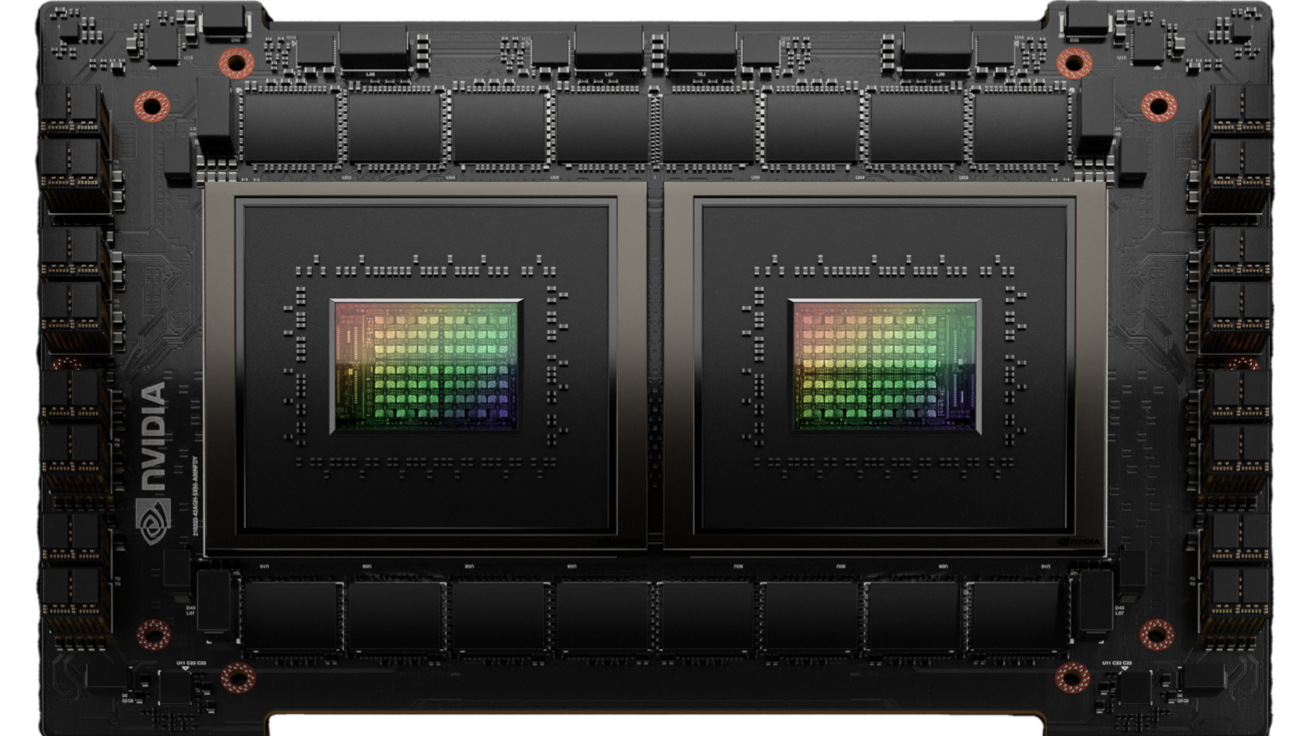
Before we unpack the NVIDIA GB200’s architecture, we should note that there are different configurations of the GB200. For example, there is the GB200 NVL72, GB200 NVL36, and so on. For simplicity, we’ll focus on the GB200 Grace Blackwell superchip, the primary component of all GB200 GPUs.
 Source: NVIDIA
The reason it is called a superchip is that it is made up of two NVIDIA B200 GPUs and a GraceTM CPU. The combination relies on the strengths of both GPUs and CPUs, with the GPUs handling parallel processing tasks and the CPU managing complex logic and data flow.
We won’t cover the B200 in great detail here, as we did that extensively in our previous article on the Blackwell GPUs. Instead, we will focus on other parts of the architecture that we have not discussed before, and we’ll begin with the Grace CPU.
NVIDIA Grace CPU superchip
Let's take a closer look at the Grace CPU superchip and its key features.
The NVIDIA Grace CPU superchip is made up of two NVIDIA Grace CPUs, among other components. While traditional CPUs focus solely on general-purpose processing, Grace is designed with AI and high-performance computing in mind, meaning it's built to handle the massive datasets and complex calculations common in those fields.
Grab your geek hat —this section takes a closer look at the Grace CPU superchip’s components!:
Dual Grace CPUs:
Each Grace CPU within the superchip has 72 Arm Neoverse V2 cores, bringing its core count to 144. The Arm Neoverse is a group of 64-bit ARM processor cores that are intended for data centers, edge computing, and high-performance computing.
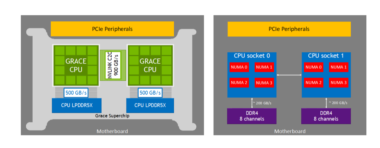 Comparison of the Grace CPU Superchip with NVLink-C2 compared to traditional server architecture. Source: NVIDIA
Since it has two CPU chips (like in the above image), it uses an NVLink chip-to-chip connection. NVLink is NVIDIA's high-speed interconnect technology that provides a 900 GB/s direct connection between the chips. It enables ultra-fast communication and data sharing, which increases the superchip's overall performance.
Scalable coherency fabric (SCF):
To keep all the chip’s cores working together efficiently, NVIDIA used Scalable Coherency Fabric (SCF). SCF is like a high-speed network that connects everything within the Grace CPU superchip.
It's a mesh fabric and distributed cache architecture designed to scale cores and bandwidth. Put simply, it can handle the immense amount of data flowing between the CPU cores, NVLink-C2C, memory, and system I/O.
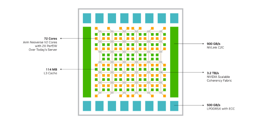 NVIDIA Grace CPU and the NVIDIA Scalable Coherency Fabric, which join the Neoverse V2 cores, distributed cache, and system IO in a high-bandwidth mesh interconnect. Source: NVIDIA
SCF provides over 3.2 TB/s of total bi-section bandwidth. A good analogy is having a massive highway system with multiple lanes and interchanges for smooth and efficient traffic flow. Apologies in advance; there will be a lot of traffic-related analogies in this piece.
The CPU cores and SCF cache partitions are distributed throughout this mesh network, while Cache Switch Nodes route data through the fabric and act as interfaces between the CPU, cache memory, and system I/Os.
A Grace CPU Superchip also has 228 MB of distributed L3 cache across the two chips, acting as a high-speed storage area, allowing the CPU to quickly access frequently used data.
Memory partitioning and monitoring (MPAM):
Another key feature of the Grace CPU superchip is its support for Arm's Memory Partitioning and Monitoring (MPAM). MPAM allows for fine-grained control over how memory resources are allocated and used. It’s a system that ensures each application or task gets the resources it needs without interfering with others.
The NVIDIA-designed SCF Cache supports partitioning of cache capacity, input and output (I/O), and memory bandwidth using MPAM. This means you can allocate specific portions of the cache and memory to different jobs, providing performance isolation and preventing one job from hogging resources and impacting others.
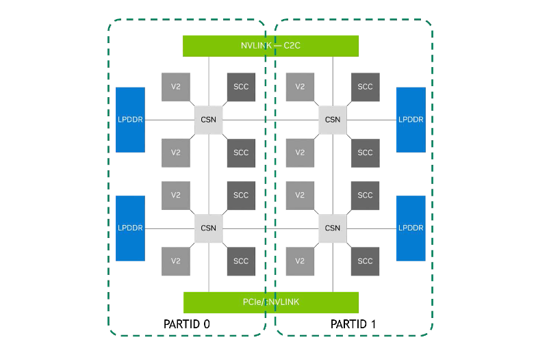 Grace CPU memory, SCF cache, PCIe, NVLink, and NVLink-C2C can be partitioned for cloud-native workloads. Source: NVIDIA
It also supports the use of MPAM performance monitor groups (PMGs) for monitoring resources, such as cache storage usage and memory bandwidth usage, allowing for detailed insights into how the CPU’s resources are being used, which enables better resource management.
LPDDR5X memory subsystem:
The Grace CPU superchip uses a memory technology designed for high performance and low power consumption called LPDDR5X. The superchip can support up to 960 GB of this server-class LPDDR5X memory.
Compared to traditional DDR memory, LPDDR5X has higher bandwidth while consuming less power, and it’s also more cost-effective and space-efficient than other high-bandwidth memory technologies like HBM2e.
The Grace CPU's LPDDR5X implementation is interesting because it's designed for resilience and reliability. It has advanced error correction and a new provisioning technique that removes the need to replace failed memory modules in the field. This makes it suitable for deployments where serviceability is hard or costly.
The lower power consumption of LPDDR5X also contributes to reduced cooling requirements and overall energy efficiency, making it a more sustainable choice for data centers and other power-constrained environments.
CPU I/O:
The Grace CPU superchip also allows connections to other devices. It uses the latest PCIe Gen 5 technology, which is like having lots of high-speed lanes for data to travel between the CPU and things like network cards, storage drives, and other components, ensuring the CPU can communicate effectively with the rest of the system and access data quickly.
Arm architecture and other features:
The Grace CPU's Neoverse V2 cores implement the Armv9.0-A architecture, one of the latest iterations of the Arm architecture, making it compatible with many existing software and libraries, including those designed for older Arm architectures.
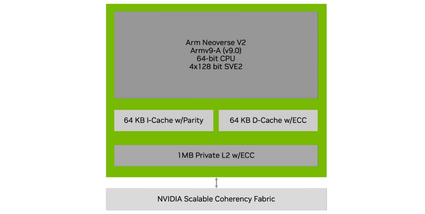 NVIDIA Grace Arm Neoverse V2 Core is the highest-performing Arm Neoverse core with support for SVE2 to accelerate key applications. Source: NVIDIA
In addition to the SVE2 vector extension mentioned earlier, the Neoverse V2 cores also support the NEON SIMD instruction set, which increases their ability to speed up different applications, including those in machine learning, genomics, and cryptography.
Also, the Grace CPU supports the Large System Extension (LSE), which provides efficient atomic operations. These operations are important for tasks that require synchronization and coordination between multiple cores, like web browsers, video editing software, operating systems (multi-threaded applications), and parallel processing.

Now, let’s do a quick rundown of the B200.
NVIDIA B200 GPU
While we won't get into every detail of the B200 GPU here for the reason we stated earlier (we covered that extensively in our previous article on Blackwell GPUs), it's worth highlighting a few key aspects that contribute to the GB200's overall performance.
The B200 has 16,896 CUDA cores and 528 Tensor Cores, and as stated earlier, these cores handle the parallel processing capabilities of GPUs. In terms of performance, the B200 can reach clock speeds of up to 1,837 MHz and can achieve approximately 62 TFLOPS of performance for single-precision calculations and 31 TFLOPS for double-precision, making it great for complex simulations and scientific computations.
Curious about how core count affects GPU performance? Check out our deep dive: NVIDIA H100 versus H200: how do they compare?
Each B200 GPU has 192GB of HBM3e memory to support its high core count and demanding workloads. HBM3e is the fastest type of memory currently available, offering a memory bandwidth of up to 8 TB/s.
The B200 also has NVIDIA's fifth-generation NVLink technology, enabling high-speed communication between GPUs with a bandwidth of up to 1.8 TB/s, allowing multiple GPUs to work together seamlessly, further boosting performance for large-scale tasks.
In essence, the B200 is a highly capable GPU that forms the foundation of the GB200's impressive performance.
NVIDIA GB200 use cases and performance benchmarks
Now that we've explored the architecture of the GB200 let's see what it can actually do. NVIDIA says it is a game-changer for AI and high-performance computing, and the benchmarks support that claim.
One of the key areas where the GB200 shines is large language model (LLM) inference—these models, which power applications like chatbots and text summarization, require immense computational resources.
In tests with a trillion-parameter LLM, the GB200 delivered 30x faster real-time throughput compared to the H100, NVIDIA's previous-generation flagship GPU, which means it can handle more requests and generate responses much quicker, leading to a smoother and more responsive user experience.
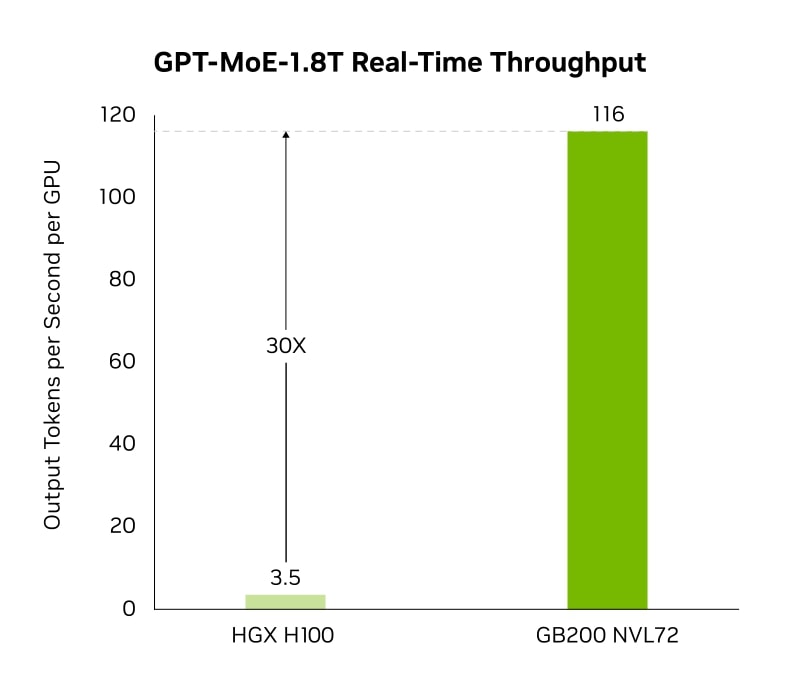 Source: NVIDIA
But the GB200 isn't just about speed; it's also about energy efficiency. In the same LLM inference benchmark, the GB200 was 25x more energy efficient than the H100. This is important now more than ever when reducing energy consumption is a major concern for data centers and other large-scale computing environments.
Another thing the GB200 is great for is database query processing. In a benchmark based on a TPC-H query, the GB200 demonstrated 18x faster performance than a comparable CPU-based system and 6x faster performance than the H100, showing its ability to speed up data analytics and data science workloads, enabling organizations to gain insights from their data more quickly.
Beyond these specific benchmarks, the GB200's architecture makes it well-suited for a wide range of other use cases, including:
- Training large language models: The GB200's massive memory capacity and high-speed interconnect allow it to handle the enormous datasets required for training LLMs, leading to faster training times and improved model accuracy.
- Scientific simulations: From climate modeling to drug discovery, the GB200 can accelerate complex simulations that require immense computational power.
- High-performance computing: The GB200's scalability allows it to be used in large-scale clusters to tackle the most demanding HPC workloads, such as those in research and scientific discovery.
Want to be among the first to try the GB200? CUDO Compute will be offering access to this cutting-edge technology soon. In the meantime, you can use our existing H100 and H200 GPUs for your AI and HPC needs. Sign up today to stay informed about the GB200's arrival and explore our current offerings! Contact us to learn more.
 Resources