Introduction
NVIDIA is a leading force in visual computing and Artificial Intelligence (AI); its flagship GPUs have become indispensable for tackling complex computational challenges in a variety of fields, including High-Performance Computing and AI. While their specifications are commonly discussed, a clear and complete picture of the various components can be hard to find and understand.

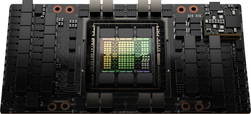
The high performance of these GPUs results from the seamless integration of their many components, each playing an important role in delivering top-tier results.
This guide offers an extensive overview of each component of an NVIDIA GPU, from architecture and Graphics Processing Clusters (GPCs) down to the individual cores. It also breaks down the intricate memory hierarchy that ensures efficient data access.
Table of Contents
Introduction
Section 1: The NVIDIA GPU architecture
- A hierarchical structure
- GPCs: The building blocks of performance
- TPCs: Powering graphics workloads
- SMs: The heart of the GPU
Section 2: CUDA cores
- What is the CUDA architecture?
- Single instruction, multiple threads (SIMT)
- Warp scheduling and execution
- Memory hierarchy and access patterns
Section 3: Specialized cores for ray tracing and AI
- RT cores: Revolutionizing real-time ray tracing
- Tensor cores: Accelerating deep learning and AI
Section 4: Memory architecture and management
- Shared memory: Collaborative computing
- L1 Cache: Fast access for frequent data
- L2 Cache: Balancing speed and capacity
- GDDR memory: High-speed data transfer
- Memory controller and interface: Managing external access
Section 5: Display and output technologies
- Raster engine: From polygons to pixels
- ROPs: Finalizing the image
- Display controller: Sending signals to the screen
- Video output ports: Connecting to monitors and TVs
Section 6: Multi-GPU systems and communication
- NVLink: High-speed interconnect
- Scalability and performance benefits
- Applications in high-Performance computing
Section 1: The NVIDIA GPU architecture
NVIDIA GPUs are designed with a hierarchical structure that allows for efficient processing of complex graphics and computational workloads. This structure can be visualized as a pyramid, with each level representing a different level of organization.
The grid is at the top of the hierarchy, representing the entire GPU and its resources. Here is how it looks:
 Source: The Next Platform
Let’s break down each component of the grid:
Graphics processing cluster (GPC)
GPCs represent a high level of organization within a GPU. They are critical for distributing workloads and managing resources across the chip. Each GPC operates relatively independently and includes its own texture processing clusters (TPCs), streaming multiprocessors (SMs), and shared resources, enabling efficient workload distribution and resource management.
The number of GPCs in a GPU varies depending on the specific model and its intended purpose. High-end GPUs designed for demanding tasks such as gaming, professional rendering, and complex computational workloads typically feature more GPCs to handle greater parallel processing demands. Conversely, lower-end GPUs, which are built for less intensive tasks, have fewer GPCs.
 Source: NVIDIA
This architectural design allows GPUs to scale performance efficiently according to the requirements of different applications and workloads. Now, let’s discuss the TPC.
Texture processing cluster (TPC)
TPCs are responsible for executing the core graphics workloads that make up the visual experience we see on our screens. They handle tasks such as:
- Vertex shading: Transforming 3D vertex coordinates into 2D screen coordinates.
- Texture mapping: Applying textures (images) to 3D models.
- Rasterization: Converting polygons into pixels for display.
Each TPC contains multiple SMs, which are the workhorses of the GPU, executing these tasks in parallel. They also contain the following:
 Source: DMST
Texture units:
These units handle tasks related to texture mapping, such as fetching texture data from memory, filtering, and applying textures to pixels or vertices. They ensure that textures are mapped correctly onto 3D models to create detailed and realistic images.
L1 cache:
A small, fast memory cache that stores frequently accessed texture data and instructions. This helps reduce latency and improves the efficiency of texture processing operations.
Shared memory:
- TPCs use shared memory to allow efficient data sharing among the texture units and SMs within the cluster. This shared memory is important for high-performance texture mapping and filtering operations.
Special function units (SFUs):
SFUs within TPCs are specifically optimized for texture mapping and rendering operations. They handle complex mathematical functions but focus more on tasks required for texture processing.
Raster engine:
The raster engine converts vector graphics (such as 3D models) into raster images (pixels). It plays a crucial role in the final stages of rendering, determining how textures are applied to individual pixels on the screen.

Texture caches:
These caches store texture data close to the texture units to minimize the time required to fetch this data from the main memory. They help speed up the texture mapping process by reducing memory access latency.
Next in the hierarchical structure is the Streaming Multiprocessors.
Streaming multiprocessors (SMs)
SMs are the fundamental processing units within the GPU. The number of SMs in a GPU is a key factor in determining its overall performance. For example, the RTX A5000, which is a general-purpose GPU, has 64 SMs, while the NVIDIA H100, which is optimized for deep learning, has 168 SMs. Here's a detailed breakdown of its components:
Instruction cache (I-Cache): Stores instructions to be executed by the SM, allowing for quick access and reducing latency by keeping frequently used instructions close to the execution units.
Multi-threaded issue (MT issue): Handles the dispatch of instructions to various execution units within the SM. It manages multiple threads simultaneously, optimizing the use of available computational resources.
Constant cache (C-cache): This cache stores constant data that doesn’t change over the course of execution. It allows for quick access to these constant values by the threads.
 Source: NVIDIA
Streaming processors/CUDA cores (SP): SPs, also known as CUDA Cores, are the cores within the SM responsible for executing most of the arithmetic operations (e.g., floating-point and integer operations). Multiple SP units enable parallel processing of instructions.
Special function units (SFU): SMs also have SFUs that handle more complex mathematical functions like trigonometric calculations, exponentials, and other special functions that are more computationally intensive than standard arithmetic operations.
Double precision units (DP): These units handle double-precision floating-point operations, which are essential for applications requiring high numerical precision, such as scientific computations and simulations.
Shared memory: Like TPC, SMs also use shared memory, a fast on-chip memory accessible by all threads within an SM. It allows for efficient data sharing and coordination among threads, significantly speeding up computations that require frequent data exchanges.
An SM in modern GPUs often contains additional cores and specialized units, which could include:
- L1 cache: A small, fast memory cache that stores frequently accessed data and instructions close to the SM cores to reduce access times.
- Registers: High-speed storage locations within each SM are dedicated to storing temporary data for active threads, allowing for rapid access during computations.
- Tensor cores: Specialized for deep learning and AI tasks, performing matrix operations essential for training and inference in neural networks.
- Ray tracing cores (RT Cores): Dedicated to handling ray tracing calculations, providing real-time rendering of realistic lighting, shadows, and reflections.
Each SM in a GPU integrates these components to execute a wide range of parallel processing tasks efficiently, balancing general-purpose computation with specialized processing for graphics, AI, and other demanding workloads.
In the following sections, we will dive deeper into the individual components of the SM, exploring how CUDA cores, RT cores, tensor cores, and shared memory work together to deliver the impressive performance that NVIDIA GPUs are known for.
Section 2: CUDA cores
NVIDIA GPUs derive exceptional computational power from multiple CUDA cores. These cores are the building blocks of parallel processing on the GPUs, enabling them to excel at tasks that demand massive computational throughput.
Here's a breakdown of the key components found within a typical CUDA core:
Arithmetic logic unit (ALU):
- Integer unit: Performs integer arithmetic operations (addition, subtraction, multiplication, division) on integer data types.
- Floating-point unit (FPU): Performs floating-point arithmetic operations (addition, subtraction, multiplication, division) on floating-point data types (e.g., single-precision FP32 and half-precision FP16).
Register file:
- Registers: A small set of high-speed storage locations within the CUDA Core for holding operands (input data) and results of computations. These registers are crucial for fast access to data during calculations.
Instruction decoder:
- Decodes instructions: Takes the incoming machine code instructions and decodes them into micro-operations that the ALU can execute.
Control logic:
- Controls execution: Manages the flow of instructions and data through the CUDA Core, ensuring that operations are performed in the correct sequence and that results are stored correctly.
Load/Store unit:
- Memory access: Handles loading data from memory into registers and storing results back to memory. This unit is responsible for interacting with the GPU's memory hierarchy (shared memory, L1 cache, global memory).
 Source: thancomputer
Additional components (optional):
- Special function unit (SFU): Some CUDA Cores may have a dedicated SFU for accelerating specific mathematical functions like sine, cosine, exponential, reciprocal, etc.
- Branch unit: Handles conditional branching instructions, allowing the CUDA Core to take different execution paths based on the results of comparisons.
Here's how CUDA cores work:
The fundamental unit of execution on a GPU is a thread. Each CUDA core within a streaming multiprocessor (SM) can execute one thread at a time. Threads are organized into groups of 32 called warps, which are scheduled and executed concurrently on an SM.
Threads can also be grouped into larger units called blocks, which enable cooperation and data sharing among threads. A block is assigned to a single SM, and the threads within that block share resources on the SM, including registers and shared memory. If a block has more threads than the SM has CUDA cores, the threads are divided into warps, and the warps are scheduled for execution as CUDA cores become available.
CUDA cores operate under the single instruction, multiple threads (SIMT) architecture, meaning that all 32 threads within a warp execute the same instruction in parallel but on different data elements. This maximizes the single instruction, multiple data (SIMD) parallelism, where a single instruction operates on multiple data points simultaneously, allowing for efficient processing of large workloads.
The GPU's scheduler in the GPC is responsible for assigning warps to available SMs for execution. When a warp encounters a long-latency operation, such as memory access, the scheduler can switch to another warp that is ready to execute, preventing latency and maximizing throughput. This dynamic scheduling ensures that the GPU's resources are utilized efficiently, even when dealing with tasks with varying execution times.
The number of CUDA cores in a GPU can range from hundreds to thousands, depending on the GPU model and its intended use case. In addition to the standard CUDA cores, modern NVIDIA GPUs feature specialized cores designed for specific tasks. Let's delve into these specialized cores and their roles in enhancing the GPU's capabilities.
Section 3: Specialized cores for ray tracing and AI
While CUDA cores form the backbone of GPU processing, modern NVIDIA GPUs have evolved to include specialized cores designed to accelerate specific workloads. These specialized cores, namely RT cores and tensor cores, have revolutionized real-time ray tracing and artificial intelligence applications, pushing the boundaries of what's possible in graphics and computing.
First, we will talk about the RT cores.
RT cores
Ray tracing is a rendering technique that simulates the physical behavior of light to produce incredibly realistic images. However, ray tracing is computationally intensive, and traditional rendering methods often struggle to achieve real-time ray tracing in interactive applications like games.
NVIDIA's RT cores are dedicated hardware units that accelerate ray tracing calculations. They are optimized for ray-triangle intersection tests, which are fundamental to ray-tracing algorithms. By offloading these computationally demanding tasks from the CUDA cores, RT Cores significantly improve the performance and efficiency of ray tracing, enabling real-time ray-traced graphics in games and other applications.
 Source: NVIDIA
RT cores have opened up a new era of visual realism, allowing for accurate lighting, shadows, reflections, and global illumination effects that were previously impossible to achieve in real time.
Here is a breakdown of its components:
RT cores (Ray tracing cores):
- Ray generation units: These units are responsible for efficiently generating light rays. They calculate the origin and direction of each ray based on camera parameters, scene information, and other factors.
- Ray-triangle intersection units: These units perform rapid ray-triangle intersection tests to determine if a ray intersects with a triangle in the scene geometry. This is a fundamental operation in ray tracing for determining object visibility and lighting calculations.
 Source: NVIDIA
- Bounding volume hierarchy (BVH) traversal units: These units efficiently navigate through BVHs, which are hierarchical data structures that accelerate ray-object intersection tests. They quickly identify which parts of the scene a ray might intersect with, reducing the number of intersection tests needed.
- Ray payload Units: These units manage the payload data associated with each ray, which includes information about the ray's origin, direction, and other properties that are needed for subsequent calculations like shading and material interactions.
Here is how the RT cores work in video editing:
Scene preprocessing (Before ray tracing starts):
- Acceleration structure building (BVH construction): Before any rays are cast, the scene geometry is analyzed and organized into a hierarchical structure called a Bounding Volume Hierarchy (BVH). This step is often performed on the CPU and doesn't directly involve RT Cores. However, the BVH is crucial for accelerating subsequent ray-object intersection tests.
Ray generation:
- RT core task: RT cores initiate the ray tracing process by generating multiple rays from the camera or light sources for indirect lighting. These rays are cast into the scene to simulate how light would travel in the real world.
- Key action: The RT cores calculate the origin and direction of each ray based on camera parameters like position, orientation, field of view, and potentially other factors like depth of field or motion blur.
Ray-scene intersection testing:
- RT core task: RT cores use the BVH to determine which objects each ray might intersect within the scene. They traverse the BVH hierarchy, starting with the largest bounding boxes and progressively moving to smaller ones, quickly eliminating irrelevant parts of the scene.
- Key action: The RT cores perform rapid ray-bounding box intersection tests to narrow down the potential candidates for ray-object intersection. They then perform more detailed ray-triangle intersection tests (if the scene is represented using triangles) to determine the exact point of intersection.
 Source: NVIDIA
The RT cores' hardware is specifically designed to accelerate these intersection tests and BVH traversal algorithms, significantly reducing the time it takes to find potential intersections compared to traditional CUDA cores or CPUs.
Shading:
- RT core task (Indirect lighting): If indirect lighting (light bouncing off multiple surfaces) is being calculated, RT Cores may generate secondary rays (reflection, refraction, shadow rays) from the intersection points to determine how light contributes to the final color of a pixel.
- Key action: RT cores calculate the direction of secondary rays and recursively continue the ray tracing process, potentially involving multiple light bounces.
Additional features:
- RT core task (optional): Depending on the complexity of the ray tracing implementation, RT cores might also handle other tasks like denoising (reducing noise in the rendered image) or global illumination (calculating lighting effects across the entire scene).
Note:
The CUDA cores are still actively involved throughout the ray tracing process. They handle tasks that are not specifically optimized for RT cores, such as:
- Shading calculations (Direct lighting): Computing the color of a pixel based on material properties, light sources, and other factors.
- Post-processing: Applying additional visual effects or filters to the rendered image.
While RT cores handle ray tracing, tensor cores are responsible for deep learning operations; let's discuss how they work.
Tensor cores
NVIDIA's Tensor cores are specialized processing units designed to accelerate deep learning operations. They are optimized for performing matrix multiplications and convolutions, which are fundamental building blocks of deep neural networks. Tensor cores can execute these operations with mixed precision, using a combination of single-precision and half-precision floating-point numbers, to significantly increase throughput without sacrificing accuracy.
 Source: NVIDIA
Here are the components of tensor cores:
Matrix multiply-accumulate (MMA) units: These are the core computational units within tensor cores. Each MMA unit can perform a 4x4 matrix multiply-accumulate operation in a single clock cycle. Multiple MMA units work together in parallel to accelerate large matrix operations.
Warp schedulers: These units schedule and manage the execution of warps (groups of threads) on the tensor cores. They ensure that the MMA units are kept busy and that the data flow is optimized for efficient computation.
Registers and Shared memory: Tensor cores have access to high-speed registers and shared memory for storing intermediate results and data shared among threads within a warp.
Mixed-precision support: Tensor cores support mixed-precision computing, meaning they can perform calculations using different numerical formats (e.g., FP16, FP32, INT8, INT4). This flexibility balances computational speed and accuracy, as deep learning models often don't require extremely high precision for all operations.
 Source: NVIDIA
Specialized units (Optional): Newer generations of tensor cores may include additional specialized units, such as:
- Sparsity engines: These units accelerate operations on sparse matrices with many zero elements.
- Transformer engines: These units are optimized to accelerate the attention mechanisms in transformer-based models, commonly used in natural language processing.
Let's break down how tensor cores work in a step-by-step fashion, highlighting their role in accelerating matrix operations that are fundamental to deep learning and AI:
1. Input data preparation:
- Data loading: The input data, typically in matrices (e.g., representing images, text, or other numerical features), is loaded into the GPU's memory.
- Data conversion (optional): If the input data is in a higher precision format like FP32 (32-bit floating point), it might be converted to a lower precision format like FP16 (16-bit floating point) to use the mixed-precision capabilities of Tensor Cores. This step is optional and depends on the specific deep learning framework and model.
2. Matrix operation scheduling:
- Operation identification: The deep learning framework identifies the matrix multiplication and accumulation (MMA) operations that need to be performed.
- Task scheduling: The framework schedules these MMA operations on the available tensor cores.
3. Tensor core operation:
- Data fetch: Tensor cores fetch the relevant data elements (matrix values) from the GPU's memory.
- Matrix multiplication: Each tensor Core performs a 4x4 matrix multiplication operation on the fetched data. This means it multiplies two 4x4 matrices and produces a 4x4 result matrix.
- Accumulation: Tensor cores accumulate the results of multiple 4x4 matrix multiplications to compute the final result of a larger matrix multiplication operation.
- Output: The results of the MMA operation are stored back in the GPU's memory.
 Source: NVIDIA
4. Mixed-precision handling (optional):
This step doesn’t happen with all GPUs and AI models, but if it does, here is how it works:
- FP16 accumulation: If the input data was converted to FP16, the accumulation of results is typically done in FP16 for faster computation.
- FP32 conversion: After the accumulation in FP16, the final result may be converted back to FP32 for higher accuracy if required by the deep learning model.
5. Iteration and completion:
- Repeated execution: Steps 3 and 4 are repeated for all the scheduled MMA operations until the entire deep-learning computation is complete.
Tensor Cores have become essential tools for accelerating deep learning research and development. They have enabled larger and more complex training models, leading to breakthroughs in various domains. For example, in natural language processing, Tensor Cores have powered the development of large language models like GPT-3, which can generate human-like text, translate languages, and even write code.
The combination of RT Cores and Tensor Cores in NVIDIA GPUs has ushered in a new era of accelerated computing, enabling real-time ray tracing and faster AI training and inference.
Section 4: Memory architecture and management
Efficient memory management is crucial for achieving high performance on NVIDIA GPUs. In this section, we delve into the intricate memory architecture that enables NVIDIA GPUs to handle massive amounts of data while minimizing latency and maximizing throughput. We'll explore shared memory, L1 cache, L2 cache, GDDR memory, and the role of memory controllers and interfaces in orchestrating data movement.
Shared memory
Shared memory is a small, low-latency memory region accessible by all threads within a thread block. It serves as a communication and synchronization mechanism between threads, allowing them to exchange data and coordinate their execution efficiently. Shared memory is on-chip and resides within the Streaming Multiprocessor (SM), making it significantly faster to access than the GPU's global memory.
 Source: NVIDIA
By using shared memory, threads can avoid redundant data transfers from global memory, reducing latency and improving performance. For example, threads working on neighboring pixels in image processing can share data in shared memory, eliminating the need to fetch the same data from global memory multiple times.
L1 cache
L1 cache is a small, high-speed memory cache located within each SM. It stores frequently accessed data and instructions, reducing the need to fetch them from slower memory levels like shared or global memory. L1 cache is typically divided into separate instruction cache and data cache, allowing concurrent access to instructions and data.
The L1 cache helps in reducing memory access latency and improving overall performance. By caching frequently used data and instructions, the GPU can avoid costly memory accesses, ensuring that the CUDA cores are fed with a steady stream of data and instructions to keep them busy.
L2 cache
L2 cache is a larger, slower cache shared by all SMs within a GPC. It serves as an intermediate level between the L1 cache and global memory, storing data that is not frequently accessed enough to be kept in the L1 cache but is still more frequently accessed than data in global memory.
The L2 cache helps to reduce the number of accesses to global memory, which can be a bottleneck for performance. By caching data shared across multiple SMs, the L2 cache reduces contention for global memory bandwidth and improves overall throughput.
Memory
Memory: GDDR and HBM
There are two types of memory commonly found in the latest NVIDIA GPUs. Let's discuss each:
GDDR memory
Graphics Double Data Rate (GDDR) memory is a high-speed memory designed specifically for GPUs. It offers high bandwidth and low latency, making it ideal for storing and transferring the large amounts of data used in graphics and compute applications.

GDDR memory is typically connected to the GPU through a wide memory interface, allowing for parallel data transfer. The latest generations of GDDR memory (GDDR6, GDDR6X, and GDDR7) offer even higher bandwidth and lower power consumption, further improving the performance of NVIDIA GPUs. However, GDDR memory does have limitations in terms of maximum achievable bandwidth.
High bandwidth memory (HBM)
High Bandwidth Memory (HBM) is a type of high-performance memory that addresses the bandwidth limitations of GDDR. It offers significantly higher bandwidth compared to GDDR memory by stacking multiple memory dies vertically and connecting them using through-silicon vias (TSVs).

HBM also has a wider interface, further increasing the data transfer rate. This makes HBM ideal for applications that require massive amounts of data to be transferred quickly, such as deep learning, scientific simulations, and high-performance computing.
HBM's vertical stacking and wide interface provide a shorter signal path and more data channels, contributing to its superior bandwidth. However, HBM is more expensive to manufacture due to its complex 3D structure and the use of TSVs.
Why GDDR and HBM Coexist:
- Cost: GDDR memory is more cost-effective to manufacture, making it suitable for consumer-grade GPUs where affordability is a concern. HBM, due to its complexity, is more expensive.
- Power consumption: GDDR memory typically consumes more power than HBM. This can be a limiting factor in power-constrained environments like laptops or mobile devices, where GDDR is preferred.
- Performance requirements: While HBM offers superior bandwidth, GDDR memory is still capable of delivering high performance for many applications. This makes GDDR a viable option for gaming GPUs and other consumer-oriented devices.
Memory controller and interface
The memory controller is a crucial component of the GPU architecture. It manages the flow of data between the GPU and the memory (either GDDR or HBM). The memory controller schedules memory accesses, ensures data integrity, and optimizes memory bandwidth utilization.
The memory interface is the physical connection between the GPU and the memory. It consists of multiple data channels that allow for parallel data transfer, maximizing the bandwidth between the GPU and memory.
Efficient memory management is essential for achieving optimal performance on NVIDIA GPUs. By understanding the roles of shared memory, L1 cache, L2 cache, GDDR memory, HBM memory, and the memory controller and interface, you can gain valuable insights into how data is organized and accessed within the GPU, ultimately leading to better application performance.
Section 5: Display and output technologies
For GPUs optimized for video rendering, the final stage in the GPU pipeline involves transforming the rendered data into a visual output that we can see on our screens. This section explores the display and output technologies within NVIDIA GPUs, including the Raster Engine, Raster Operation pipelines (ROPs), Display Controller, and Video Output Ports. These components work harmoniously to ensure that the rendered images are displayed seamlessly and with high fidelity.
Raster engine
The Raster engine is responsible for converting the geometric representation of a scene (polygons, triangles, etc.) into a raster image (pixels). The process involves determining which pixels on the screen are covered by each polygon and assigning the corresponding color and depth values to those pixels. The Raster Engine performs this task for every frame rendered, ensuring that the final image is a faithful representation of the 3D scene.
Key functions of the raster engine include:
- Triangle setup: Preparing the triangle data for rasterization, including calculating edge slopes and determining pixel coverage.
- Pixel shading: Calculating the final color of each pixel based on lighting, material properties, and other factors.
- Z-buffering: Maintaining a depth buffer to determine which objects are visible and which are occluded by other objects in the scene.
- Anti-aliasing: Smoothing out jagged edges of polygons to improve image quality.

The Raster engine's performance helps achieve high frame rates and smooth visuals in games and other real-time applications. NVIDIA GPUs feature advanced raster engines that are optimized for high throughput and efficiency, enabling them to handle complex scenes with millions of polygons at high frame rates.
Raster operations pipelines
Raster operations pipelines (ROPs) are responsible for the final stages of pixel processing before the image is displayed on the screen. They perform tasks such as:
- Blending: Combining the colors of multiple overlapping objects to create transparency and other visual effects.
- Depth testing: Determining which pixels are visible based on their depth values.
- Anti-aliasing: Further smoothing out edges and reducing visual artifacts.
- Gamma correction: Adjusting the brightness and contrast of the image for optimal display.
- Display output formatting: Preparing the final pixel data for transmission to the display.
 Source: Research Paper
The number of ROPs in a GPU can affect its fill rate, which is the rate at which it can render pixels. High-end GPUs typically have more ROPs, allowing them to handle higher resolutions and more complex scenes with ease.
Display controller
The Display controller is the interface between the GPU and the display device. It receives the processed pixel data from the ROPs and converts it into a format that the display can understand. The Display controller also handles tasks such as:
- Resolution and refresh rate management: Setting the display resolution and refresh rate based on user preferences and monitor capabilities.
- Color space conversion: Converting the image data from the GPU's internal color space to the color space used by the display.
- Scaling and rotation: Adjusting the image size and orientation to fit the display.
- Video output signal generation: Generating the appropriate video signal (e.g., DisplayPort, HDMI) for transmission to the display.
Modern display controllers support high resolutions, high refresh rates, and various display technologies such as G-Sync and High Dynamic Range (HDR), delivering smooth, vibrant, and immersive visuals.
Video output ports
Video Output Ports are the physical connectors on the GPU that allow it to be connected to various display devices. These ports can include:
- DisplayPort: A high-speed digital interface that supports high resolutions, high refresh rates, and features like G-Sync and HDR.
- HDMI: A popular consumer interface that supports high resolutions and audio transmission.
- DVI: An older digital interface that is still used in some legacy displays.
The availability of different video output ports provides flexibility for connecting NVIDIA GPUs to a wide range of displays, from high-end gaming monitors to large-screen TVs.

Together, the raster engine, ROPs, display controller, and video output ports form a sophisticated pipeline that transforms the raw data generated by the GPU into the stunning visuals that we see on our screens. Understanding how these components work together is essential for appreciating the intricacies of GPU technology and the impressive visual experiences it enables.
Section 6: Multi-GPU systems and communication
Modern computing demands often exceed the capabilities of a single GPU. To tackle these challenges, NVIDIA has developed technologies that enable the seamless integration and communication of multiple GPUs within a system. This section focuses on NVLink, a high-speed interconnect technology that facilitates efficient data transfer and collaboration between GPUs, leading to significant scalability and performance benefits in various high-performance computing applications.
NVLink: High-speed interconnect
NVLink is a high-bandwidth, energy-efficient interconnect technology developed by NVIDIA to enable direct communication between GPUs and, in some cases, between GPUs and CPUs. Unlike traditional PCIe (Peripheral Component Interconnect Express) connections, which have limited bandwidth and introduce latency, NVLink provides a direct and high-speed path for data exchange between GPUs.

NVLink operates at much higher data rates than PCIe, allowing for rapid transfer of large datasets and synchronization between GPUs. This enables applications to leverage the combined processing power of multiple GPUs to achieve unprecedented performance levels.
Key features of NVLink include:
- High bandwidth: NVLink offers significantly higher bandwidth than PCIe, allowing for faster data transfer between GPUs.
- Low latency: NVLink's direct connection minimizes latency, enabling efficient communication and synchronization between GPUs.
- Scalability: NVLink allows for the connection of multiple GPUs in a variety of topologies (e.g., mesh, ring), providing flexibility and scalability for different system configurations.
- Energy efficiency: NVLink is designed to be energy-efficient, minimizing power consumption while delivering high performance.
Scalability and performance benefits
NVLink's high bandwidth and low latency enable multi-GPU systems to achieve significant scalability and performance benefits. By efficiently distributing workloads across multiple GPUs and enabling them to communicate directly, NVLink can accelerate a wide range of applications, including:
- Deep learning: Training and inference of large deep learning models can be dramatically accelerated by leveraging the combined computational power of multiple GPUs connected through NVLink.
- High-performance computing (HPC): Scientific simulations, computational fluid dynamics, and other HPC applications benefit from NVLink's ability to quickly transfer large datasets and synchronize calculations between GPUs.
- Professional visualization: Applications like 3D rendering, video editing, and visual effects can achieve real-time or near-real-time performance with the help of NVLink's fast data transfer between GPUs.
Applications in high-performance computing
NVLink has found widespread adoption in high-performance computing environments, where the need for massive computational power is paramount. Data centers and research institutions utilize NVLink to build powerful multi-GPU clusters that can tackle complex problems that were previously intractable.
Some notable applications of NVLink in high-performance computing include:
- Climate modeling: Simulating complex climate models requires enormous computational resources. NVLink-enabled GPU clusters can accelerate these simulations, leading to more accurate predictions and a better understanding of climate change.
- Drug discovery: Identifying potential drug candidates involves analyzing vast amounts of data. NVLink helps to speed up this process, potentially leading to faster drug development.
- Autonomous vehicles: Training and deploying the complex algorithms that power autonomous vehicles require significant computational power. NVLink-enabled GPUs accelerate this process, bringing us closer to a future of safer and more efficient transportation.
By facilitating seamless communication and collaboration between multiple GPUs, NVLink has become a critical technology for unlocking the full potential of GPUs in high-performance computing. As the demands for computational power continue to grow, NVLink will play an increasingly important role in pushing the boundaries of what's possible.
Final thoughts
NVIDIA’s GPU components are improving with each new generation, and the introduction of the Blackwell series is the latest iteration. While this guide has provided a comprehensive overview of the core components found in most modern NVIDIA GPUs, Blackwell introduces new features like FP4 precision as well as enhancements to existing capabilities.
Although not covered in this guide, FP4 precision is a groundbreaking development. It represents a further reduction in the number of bits used to represent floating-point numbers, allowing for faster calculations and reduced memory requirements.
While FP4 may sacrifice some numerical precision, it opens up new possibilities for accelerating AI inference workloads, where speed often outweighs the need for extreme accuracy.
As stated previously, from a practical implication point of view, Blackwell GPUs can address previously computationally expensive problems like the high-fidelity climate simulations undertaken by Earth-2.
Follow our blog to learn more about the latest NVIDIA hardware. We offer competitive prices for NVIDIA GPUs like the H100 and H200. Also, with CUDO Compute, you can upgrade to the NVIDIA B100 as soon as it is released. Get started today.